Quartz Wave Plates
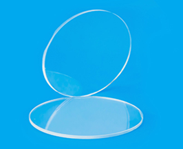
Quartz Wave Plates (or Phase Retardation Plates) are optical elements capable of altering the phase of polarized light waves passing through them.
Processing Capacity:
Items | Specification |
Overall dimension | customized |
Wave Plate Type | 0-level/multi-level wave plate |
Wavefront Distortion | λ/10 @ 632.8nm |
Phase Retardation Accuracy | λ/500 |
Parallelism | ≥1 arc second |
Surface Quality | 10-5 |
Optical Glass Plates
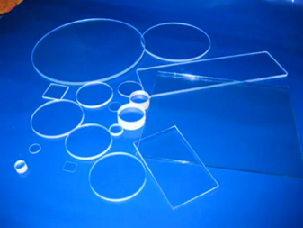
Optical glass plates are primarily used as window plates for protecting and adjusting optical systems' spectral bands, or as filter plates to select desired radiation bands.
Processing Capacity:
Items | Specification |
Overall dimension | customized |
Wavefront Distortion | λ/10 @632.8nm |
Ra | ≤1nm |
Parallelism | ≥1 arc second |
Surface Quality | 10-5 |
Optical Lithium Niobate(LN) Wafers
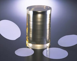
Optical Lithium Niobate wafers are significant photoelectric materials, exhibiting excellent electro-optic, acousto-optic, nonlinear optical, and piezoelectric properties. They are widely utilized in various photoelectric integrated devices due to their unique optical and electrical properties.
Processing Capacity:
Items | Specification |
Overall dimension | 1-inch to 8-inch |
Thickness | ≥0.2mm±0.01mm |
Ra | ≤1nm |
TTV | ≤2.5μm (remove edge 3mm) |
Flatness | ≤10N |
Surface Quality | 10-5 |
Quartz Wafers

Quartz wafers are circular thin plates made of glass materials, primarily used as optical coating substrates or for the fabrication of micro-optical elements, integrated optics, and photonic chips. Its thickness is usually less than 1 mm, and the size is similar to that of silicon wafers, which are divided into 6 inches, 8 inches, 12 inches and other specifications.
Processing Capacity:
Item | Specification |
Overall dimension | Φ100-200±0.1mm |
Thickness | ≥0.5mm±0.01mm |
Ra | ≤1nm |
Bow | ≤10μm |
TTV | ≤2μm |
Warp | ≤15μm |
Surface Quality | 10-5 |
AR Waveguide
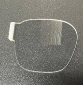
AR waveguide is a key component in augmented reality (AR) technology, which is responsible for directing image light to the user's eyes to achieve the superposition of virtual images and the real world. AR waveguide pieces will be widely used in smart glasses, vehicle AR-HUD, holographic display and other fields.
Processing Capacity:
| Item | Specification |
Overall dimension | 52*60mm |
Flatness | ≤3N |
Surface Quality | 40-20 |
Parallelism | ≤5″ |
Ra | ≤10nm |
Thin Film Lithium Niobate
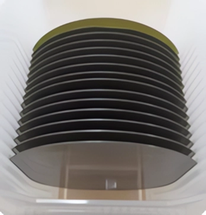
The thickness of the surface LN/LT layer of the multilayer bonding substrate is reduced to a μm-level POI (Piezoelectric on Insulator) substrate by mechanical and special processing method. It is mainly used in 5G/6G (high-end SAW filters), optical communication (thin film electro-optical modulators), sensors and other fields.
Processing Capacity:
Item | Specification | |
Wafer size | 4/6 inch | |
Film thickness | LN/LT film thickness | 1~20μm |
LN/LT film TTV | <600nm | |
Ra | <0.5nm | |

